Discontinued Products
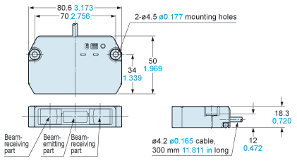
Dimensions
- Unit: mm in
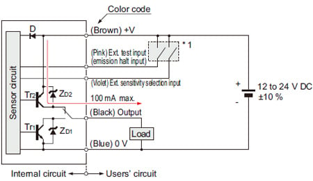
I/O Circuit and Wiring diagrams
NPN output
I/O circuit diagram
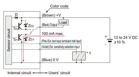
Symbols・・・D:Reverse supply polarity protection diodeZD1,ZD2:Surge absorption zener diodeTr1:NPN output transistorTr2:PNP output transistor
Wiring diagram
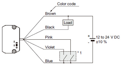
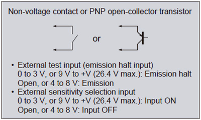
*1

PNP output
I/O circuit diagram
Symbols・・・D:Reverse supply polarity protection diodeZD1,ZD2:Surge absorption zener diodeTr1:NPN output transistorTr2:PNP output transistor
Wiring diagram
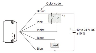
*1
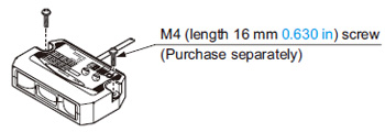
Mounting
- Set the distance between the sensor detection surface and the wafer edge to be 45 mm 1.772 in and mount the sensor so that sensing is done at an angle of 12.5° with respect to the wafer. Mount using M4 (length 16 mm 0.630 in) screws. The tightening torque should be 1.2 N·m or less. Further, although the sensing distance may change due to variation in the wafer position (wafer protrusion, orientation flat position, etc.), if it is within 5 mm 0.197 in, stable sensing is possible.
Top-view
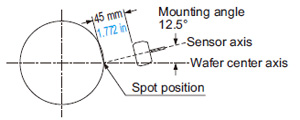
Note:If the wafer center axis and the sensor axis lie along a straight line (0°), detection is not possible. Always mount the sensor at an angle to the wafer.
Wiring
- Make sure that the power supply is off while wiring.
- Take care that wrong wiring will damage the product.
- Verify that the supply voltage variation is within the rating.
- If power is supplied from a commercial switching regulator,ensure that the frame ground (F.G.) terminal of the power supply is connected to an actual ground.
- In case noise generating equipment (switching regulator, inverter motor, etc.) is used in the vicinity of this product, connect the frame ground (F.G.) terminal of the equipment to an actual ground.
- Do not run the wires together with high-voltage lines or power lines or put them in the same raceway. This can cause malfunction due to induction.
- Extension up to total 10 m 32.808 ft, or less, is possible with 0.15 mm2, or more, cable. However, in order to reduce noise, make the wiring as short as possible.
- Make sure to use an isolation transformer for the DC power supply. If an autotransformer (single winding transformer) is used, this product or the power supply may get damaged.
- In case a surge is generated in the used power supply, connect a surge absorber to the supply and absorb the surge.
Others
- Do not use during the initial transient time (0.5 sec.) after the power supply is switched on.
- Take care that the sensor is not directly exposed to fluorescent lamp from a rapid-starter lamp, a high frequency lighting device or sunlight etc., as it may affect the sensing performance.
- Avoid dust, dirt, and steam.
- Take care that the product does not come in contact with water, oil, grease or organic solvents, such as, thinner, etc.
- Do not allow any water, oil, fingerprints, etc., which may refract light, or dust, dirt, etc., which may block light, to stick to the sensing surfaces of the sensor. In case they are present, wipe them with a clean, dust-free soft cloth or lens paper.
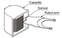
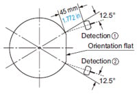
Detecting wafer having orientation flat
- When detecting a wafer having an orientation flat, mount the sensor so that a portion other than the orientation flat is detected. Further, arrange to detect the wafer from two different angles by moving the robot arm, etc., and OR the signal so obtained.
Top-view
Part description
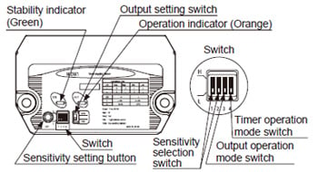
Sensitivity selection setting
- Sensitivity can be selected from four levels by appropriate setting of the sensitivity selection switch (2 bits).
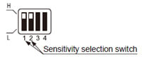
| Sensitivity selection switch | Sensitivity | |
|---|---|---|
| Maximum sensitivity (MAX) | Used for low reflectivity wafers with nitride or oxide film processing,or for thin wafers (0.3 to 0.4 mm 0.012 to 0.016 in) |
| High sensitivity (HIGH) | Sensitivity between maximum sensitivity and medium sensitivity |
| Medium sensitivity (MID) | Used for high reflectivity polished wafers, etc., or for 3 mm 0.118 in wafer pitch |
| Low sensitivity (LOW) | Lowest possible sensitivity setting |


Notes:
1)In case of 8 inch or less wafers, the wafer pitch, orientation flat or the surface condition may affect the sensing.
2)Polished wafers, etc., which have a sharp edge cannot be detected since they do not reflect the light in the light receiving direction.
External sensitivity selection input
- The external sensitivity selection input (violet) becomes ON when it is connected to 0 to 3 V, or 9 V to +V (26.4 V max.), and becomes OFF when it is kept open or connected to 4 to 8 V.
If the sensitivity is selected with the external sensitivity selection input, set the sensitivity selection switch as shown in the table below.
| Sensitivity selection switch | Ext. sensitivity selection input | Sensitivity | |
|---|---|---|---|
| 0 to 3 V, or 9 V to +V (26.4 V max.) | ON | Maximum sensitivity (MAX) |
| Open, or 4 to 8 V | OFF | Medium sensitivity (MID) | |
| 0 to 3 V or 9 V to +V (26.4 V max.) | ON | High sensitivity (HIGH) |
| Open, or 4 to 8 V | OFF | Low sensitivity (LOW) | |


Sensitivity setting
- Although this sensor has an optical system which makes it difficult for the background to affect the detection, the background may have an effect when detecting small diameter wafers. Hence, if the background gets detected, or the stability indicator (green) lights off when the cassette has no wafers, sensitivity setting should be done so that the background does not have an effect. However, the sensitivity reduces when sensitivity setting is done.
- Since the sensitivity is stored in an EEPROM when the sensitivity setting button is pressed, the setting need not be repeated when the power is switched on again. However, note that the EEPROM has a lifetime and its guaranteed life is 100,000 write operation cycles.
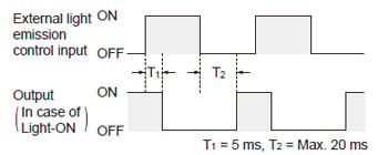
Light emission control function
- Light emission is halted when the external light emission control input (pink) is connected to 0 to 3 V, or 9 V to +V (26.4 V max.). In this case, the output turns to the dark state.
Time chart
Timer function
Using the timer operation mode switch, it is possible to select an approx. 2 ms fixed OFF-delay timer. Since the output is extended by a fixed period, it is useful when the connected device has a slow response time.
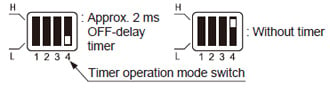
Time chart
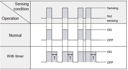
Timer period: T = Approx. 2 ms
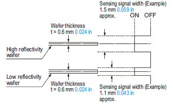
Sensing signal
(1)The sensing signal has a width larger than the thickness of the wafer.
(2)The signal width also varies with the reflectivity of the sensing edge. High reflectivity (polish, aluminum evaporated, etc.): Large signal width
Example: Wafer thickness t=0.6mm 0.024 in → Signal width 1.5 mm 0.059 in approx.
Low reflectivity (nitride or oxide film processed): Small signal width
Example: Wafer thickness t=0.6mm 0.024 in → Signal width 1.1 mm 0.043 in approx.
(3)The signal width also changes with the sensing distance or the sensing angle.
- The sensing signal which is output from the sensor is as follows:
- From the above, for determining the position of the wafer from the sensing signal, calculate the center position of the signal’s ON region, while taking into consideration the response time.
- In case of “Detecting wafer having orientation flat”, when the sensor is mounted at positions which avoid the wafer orientation flat, the pitch of a crosscondition wafer changes as shown in the figure below.
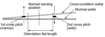
- The calculated pitch based on the wafer size is given in the table below.
| Wafer size | Normal pitch | Orientation flat length | Wafer thickness | Cross pitch (narrow) | Cross pitch (wide) |
|---|---|---|---|---|---|
| 3 inch (75mm) | 4.75mm 0.187 in | 22.2mm 0.874 in | 0.380mm 0.015 in | 1.58mm 0.062 in | 3.17mm 0.125 in |
| 4 inch (100mm) | 4.75mm 0.187 in | 32.5mm 1.280 in | 0.625mm 0.025 in | 1.54mm 0.061 in | 3.21mm 0.126 in |
| 5 inch (125mm) | 4.75mm 0.187 in | 42.5mm 1.673 in | 0.625mm 0.025 in | 1.52mm 0.060 in | 3.23mm 0.127 in |
| 6 inch (150mm) | 4.75mm 0.187 in | 57.5mm 2.264 in | 0.675mm 0.027 in | 1.43mm 0.056 in | 3.33mm 0.131 in |
| 8 inch (200mm) | 6.35mm 0.250 in | 59.3mm 2.335 in | 0.725mm 0.029 in | 2.19mm 0.086 in | 4.16mm 0.164 in |
- From the above, it is seen that, since the pitch of the cross-condition wafer reduces, the pitch resolution required for high reflectivity wafers becomes more stringent than the specified resolution of 3 mm 0.118 in. Hence, the sensing signal from two wafers may not be resolved and may become a continuous signal.
Further, the sensing signal may also change due to the sensitivity setting, the reflectivity of the wafer, and the sensing conditions (sensing distance or sensing angle).
For the above reasons, in case of wafers which have been cross-inserted, since the small cross-pitch side is similar to overlapping wafers, the sensing signal of two wafers may become a continuous signal or may get resolved. - If the orientation flat happens to get in the position of sensing, sensing is not possible in one of the two sensing positions. Therefore, if the wafer is cross-inserted, a resolved signal may not be output, and in this case, the information on the wafer position calculated from the sensing signal will be erroneous.