Panasonic Industry / Automation Controls

Applications of Relays in Electronic Circuits

Mechanical relays Selection Guide
Here is PDF of this page.

1. Relay Drive by Means of a Transistor

Connection Method

If the relay is transistor driven, we recommend using the relay on the collector side.
The voltage impressed on the relay is always full rated coil voltage, and in the OFF time, the voltage is completely zero for avoidance of trouble in use.

Collector connection

(Good)
Collector connection
With this most common connection, operation is stable.

Emitter connection

(Care)
Emitter connection
When the circumstances make the use of this connection unavoidable, if the voltage is not completely impressed on the relay, the transistor does not conduct completely and operation is uncertain.

Parallel connection

(Care)
Parallel connection
When the power consumed by the complete circuit becomes large, consideration of the relay voltage is necessary.

Countermeasures for Surge Voltage of Relay Control Transistor

If the coil current is suddenly interrupted, a sudden high voltage pulse is developed in the coil. If this voltage exceeds the breakdown voltage of the transistor, the transistor will be degraded, and this will lead to damage. It is absolutely necessary to connect a diode in the circuit as a means of preventing damage from the counter emf. As suitable ratings for this diode, the current should be equivalent to the average rectified current to the coil, and the reverse blocking voltage should be about 3 times the value of the power source voltage. Connection of a diode is an excellent way to prevent voltage surges, but there will be a considerable time delay when the relay is open. If you need to reduce this time delay you can connect between the transistor's collector and emitter a Zener diode that will make the Zener voltage somewhat higher than the supply voltage.

Take care of "Area of Safe Operation (ASO)".

Snap Action

Characteristic of Relay With Voltage Rise and Fall of Voltage

Unlike the characteristic when voltage is impressed slowly on the relay coil, this is the case where it is necessary to impress the rated voltage in a short time and also to drop the voltage in a short time.

Non-pulse signal

(No Good)
Without snap action

Pulse signal (square wave)

(Good)
Snap action

Schmitt Circuit (Snap Action Circuit)

Wave rectifying circuit

When the input signal does not produce a snap action, ordinarily a Schmitt trigger circuit is used to produce safe snap action.

Characteristic Points

  • The common emitter resistor REmust have a value sufficiently small compared with the resistance of the relay coil.
  • Due to the relay coil current, the difference in the voltage at point P when T2is conducting and at point P when T1is conducting creates hysteresis in the detection capability of Schmitt circuit, and care must be taken in setting the values.
  • When there is chattering in the input signal because of waveform oscillation, a RC time constant circuit should be inserted in the stage before the Schmitt trigger circuit. (However, the response speed drops.)

Avoid Darlington Circuit Connections.

High amplification

This circuit is a trap into which it is easy to fall when dealing with high circuit technology. This does not mean that it is immediately connected to the defect, but it is linked to troubles that occur after long periods of use and with many units in operation.

(No good)
Darlington connection

Due to excessive consumption of power,
heat is generated.
A strong Tr1 is necessary.

(Good)
Emitter connection

Tr2 conducts completely.
Tr1is sufficient for signal use.

Residual Coil Voltage

In switching applications where a semiconductor (transistor, UJT, etc.) is connected to the coil, a residual voltage is retained at the relay coil which may cause incomplete restoration and faulty operation. By using DC coils, there may be a danger of incomplete restoration, and a reduction in the contact pressure and the vibration resistance.
This is because the release voltage is 10% or more of the rated voltage, a low value compared to that for AC coil, and also there is a tendency to increase the life by lowering the release voltage.
When the signal from the transistor's collector is taken and used to drive another circuit as shown in the figure on the right, a minute dark current flows to the relay even if the transistor is off. This may cause the problems described above.

Connection to the next stage through collector

2. Relay Drive by Means of SCR

Ordinary Drive Method

For SCR drive, it is necessary to take particular care with regard to gate sensitivity and erroneous operation due to noise.

  • IGT : There is no problem even with more than 3 times the rated current.
  • RGK : 1 KΩ must be connected.
  • R, C : This is for prevention of ignition error due to a sudden rise in the power source or to noise. (dv/dt countermeasure)

Caution Points Regarding ON/OFF Control Circuits

When Used for Temperature or Similar Control Circuits

When the relay contacts close simultaneously with an AC single phase power source, because the electrical life of the contacts suffers extreme shortening, care is necessary.

  1. When the relay is turned ON and OFF using a SCR, the SCR serves as a half wave power source as it is, and there are ample cases where the SCR is easily restored.
  2. In this manner the relay operation and restoration timing are easily synchronized with the power source frequency, and the timing of the load switching also is easily synchronized.
  3. When the load for the temperature control is a high current load such as a heater, the switching can occur only at peak values and it can occur only at zero phase values as a phenomenon of this type of control. (Depending upon the sensitivity and response speed of the relay)
  4. Accordingly, either an extremely long life or an extremely short life results with wide variation, and it is necessary to take care with the initial device quality check.

3. Relay Drive from External Contacts

Relays for PC board use have high sensitivity and high speed response characteristics, and because they respond sufficiently to chattering and bouncing, it is necessary to take care in their drive.
When the frequency of use is low, with the delay in response time caused by a condenser, it is possible to absorb the chattering and bouncing.
(However, it is not possible to use only a condenser. A resistor should also be used with the condenser. )

4. LED Series and Parallel Connections

1)In series with relay

In series with relay

Power consumption:
In common with relay (Good)
Defective LED:
Relay does not operate (No good)
Low voltage circuit:
With LED, 1.5V down (No good)
No. of parts: (Good)

2)R in parallel with LED

R in parallel with LED

Power consumption:
In common with relay (Good)
Defective LED:
Relay operate (Good)
Low voltage circuit:
With LED, 1.5V down (No good)
No. of parts: R1 (Care)

3)In parallel connection with relay

In parallel connection with relay

Power consumption:
Current limiting resistor R2 (Care)
Defective LED:
Relay operate stable (Good)
Low voltage circuit: (Good)
No. of parts: R2 (Care)

5. Electronic Circuit Drive by Means of a Relay

Chatterless Electronic Circuit

Even though a chatterless characteristic is a feature of relays, this is to the fullest extent a chatterless electrical circuit, much the same as a mercury relay. To meet the requirement for such circuits as the input to a binary counter, there is an electronic chatterless method in which chattering is absolutely not permissible. Even if chattering develops on one side, either the N.O. side contacts or the N.C. side contacts, the flip flop does not reverse, and the counter circuit can be fed pulsed without a miss. (However, bouncing from the N.O. side to N.C. side must be absolutely avoided.)

Notes:  

  1. The A, B, and C lines should be made as short as possible.
  2. It is necessary that there be no noise from the coil section induced into the contact section.

Triac Drive

When an electronic circuit using a direct drive from a triac, the electronic circuit will not be isolated from the power circuit, and because of this, troubles due to erroneous operation and damage can develop easily. The introduction of a relay drive is the most economical and most effective solution. (Photo coupler and pulse transformer circuits are complicated.)
When a zero cross switching characteristic is necessary, a solid state relay (SSR) should be used.

6. Power Source Circuit

Constant Voltage Circuit

In general, electronic circuits are extremely vulnerable to such phenomena as power supply ripples and voltage fluctuations. Although relay power supplies are not as vulnerable as electronic circuits, please keep both ripples and the regulation within the specification.

  • If power supply voltage fluctuations are large, please connect a stabilized circuit or constant-voltage circuit as shown in Fig. 1.
  • If the relay power consumption is great, satisfactory results can be achieved by implementing a circuit configuration as shown in Fig. 2.

Prevention of Voltage Drop Due to Rush Current

In the circuit shown in Fig. 1, rush current flows from the lamp or capacitor. The instant the contacts close, the voltage drops and the relay releases or chatters.
In this case it is necessary to raise the transformer's capacity or add a smoothing circuit.

  • Fig. 2 shows an example of the modified circuit.
  • Fig. 3 shows a battery-powered version.

7. PC Board Design Considerations

Pattern Layout for Relays

Since relays affect electronic circuits by generating noise, the following points should be noted.

  • Keep relays away from semiconductor devices.
  • Design the pattern traces for shortest lengths.
  • Place the surge absorber (diode, etc.) near the relay coil.
  • Avoid routing pattern traces susceptible to noise (such as for audio signals) underneath the relay coil section.
  • Avoid through-holes in places which cannot be seen from the top (e.g. at the base of the relay).
  • Solder flowing up through such a hole may cause damage such as a broken seal.
  • Even for the same circuit, pattern design considerations which minimize the influence of the on/off operations of the relay coil and lamp on other electronic circuits are necessary.

Hole and Land Diameter

The hole diameter and land are made with the hole slightly larger than the lead wire so that the component may be inserted easily. Also, when soldering, the solder will build up in an eyelet condition, increasing the mounting strength. The standard dimensions for the hole diameter and land are shown in the table below.

Standard dimensions for hole and land diameter (Unit: mm)

Standard hole diameterToleranceLand diameter
0.8±0.12.0~3.0
1.0
1.23.5~4.5
1.6

Remarks

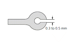
  • The hole diameter is made 0.2 to 0.5 mm larger than the lead diameter. However, if the jet method (wave type,jet type) of soldering is used,because of the fear of solder passing through to the component side, it is more suitable to make the hole diameter equal to the lead diameter +0.2mm.
  • The land diameter should be 2 to 3 times the hole diameter.
  • Do not put more than 1 lead in one hole.

Expansion and Shrinkage of Copperclad Laminates

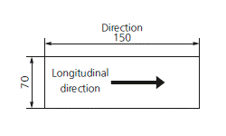
Because copperclad laminates have a longitudinal and lateral direction,the manner of punching fabrication and layout must be observed with care. The expansion and shrinkage in the longitudinal direction due to heat is 1/15 to 1/2 that in the lateral,and accordingly, after the punching fabrication, the distortion in the longitudinal direction will be 1/15 to 1/2 that of the lateral direction. The mechanical strength in the longitudinal direction is 10 to 15% greater than that in the lateral direction. Because of this difference between the longitudinal and lateral directions, when products having long configurations are to be fabricated, the lengthwise direction of the configuration should be made in the longitudinal direction, and PC boards having a connector section should be made with the connector along the longitudinal side.

Example : As shown is the drawing below, the 150 mm direction is taken as the longitudinal direction.

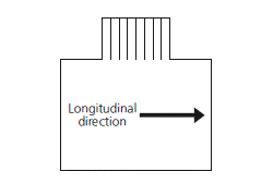
Also, as shown in the drawing below, when the pattern has a connector section, the direction is taken as shown by the arrow in the longitudinal direction

When it is Necessary to Use Hand Soldering for One Part of a Component After Dip Soldering Has Been Done

By providing a narrow slot in the circular part of the foil pattern, the slot will prevent the hole from being plugged with solder.

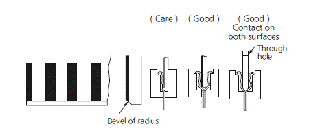
When The Printed Circuit Board Itself is Used as a Connector

  • The edge should be beveled. (This prevents peeling of the foil when the board is inserted into its socket.)
  • When only a single side is used as the connector blade, if there is distortion in the circuit board, contact will be defective. Care should be taken.

PC Board Reference Data

This data has been derived from samples of this company's products. Use this data as a reference when designing printed circuit boards.

Conductor Width

The allowable current for the conductor was determined from the safety aspect and the effect on the performance of the conductor due to the rise in saturation temperature when current is flowing. (The narrower the conductor width and the thinner the copper foil, the larger the temperature rise.) For example, too high a rise in temperature causes degradation of the characteristic and color changes of the laminate. In general, the allowable current of the conductor is determined so that the rise is temperature is less than 10°C. It is necessary to design the conductor width from this allowable conductor current.
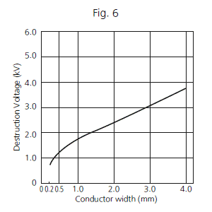
Fig. 1, Fig. 2, Fig. 3 show the relationship between the current and the conductor width for each rise in temperature for different copper foils. It is also necessary to give consideration to preventing abnormal currents from exceeding the destruction current of the conductor.
Fig. 4 shows the relationship between the conductor width and the destruction current.

Space Between Conductors

Fig. 6 shows the relationship between the spacing between conductors and the destruction voltage. This destruction voltage is not the destruction voltage of the PCB; it is the flash over voltage (insulation breakdown voltage of the space between circuits.) Coating the surface of the conductor with an insulating resin such as a solder resist increases the flash over voltage, but because of the pin holes of the solder resist, it is necessary to consider the conductor destruction voltage without the solder resist. In fact, it is necessary to add an ample safety factor when determining the spacing between conductors. Table 1 shows an example of a design for the spacing between conductors. (Taken from the JIS C5010 standards.) However, when the product is covered by the electrical products control law, UL standards or other safety standards, it is necessary to conform to the regulations.

Example of conductor spacing design

Maximum DC and AC Voltage Between Conductors (V)Minimum Conductor Spacing (mm)
0 to 500.381
51 to 1500.635
151 to 3001.27
301 to 5002.54
500 or moreCalculated at 0.00508 mm/V

Related Information

Catalog Download